


WaveShare Electronics
₹1,949.00 + 18% GST
B2B GST Credit Available
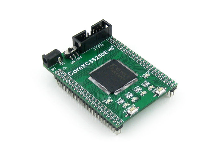
XILINX Spartan-3E FPGA Development Board - Core3S250E - XC3S250E Device
₹2,299.82
All Inclusive, Shipping Calculated at Checkout
B2B GST Credit Available
- Stock: 0 in Stock
- SKU: 01647
- Delivery Time
- Bulk & B2B RFQ
XILINX Spartan-3E FPGA Development Board - Core3S250E - XC3S250E Device
Core3S250E is an FPGA core board that features an XC3S250E device onboard, supports further expansion.
- Onboard XCF02S
- integrated FPGA basic circuit, such as clock circuit
- onboard nCONFIG button, RESET button, 4 x LEDs
- all the I/O ports are accessible on the pin headers
- onboard JTAG debugging/programming interface
- 2.54mm header pitch design, suitable for being plugged-in your application system
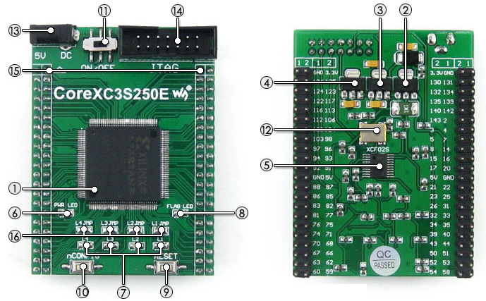
- 1. XC3S250E:the XILINX Spartan-3E FPGA device which features:
- Operating Frequency: 50MHz
- Operating Voltage: 1.15V~3.3V
- Package: QFP144
- I/Os: 80
- LEs: 250K
- RAM: 216kb
- DCMs: 4
- Debugging/Programming: supports JTAG
- 2. AMS1117-3.3, 3.3V voltage regulator
- 3. AMS1117-2.5, 2.5V voltage regulator
- 4. AMS1117-1.2, 1.2V voltage regulator
- 5. XCF02S, onboard serial FLASH memory, for storing code
- 6. Power indicator
- 7. LEDs
- 8. FPGA initialization indicator
- 9. Reset button
- 10. nCONFIG button: for re-configuring the FPGA chip, the equivalent of power reseting
- 11. Power switch
- 12. 50M active crystal oscillator
- 13. 5V DC jack
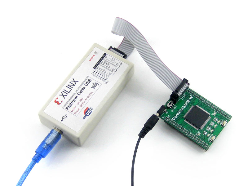
- 14. JTAG interface: for debugging/programming
- 15. FPGA pins expander, VCC, GND and all the I/O ports are accessible on expansion connectors for further expansion
- 16. LED jumpers
Programming - Debugging Interface
The Core3S250E FPGA core board integrates JTAG interface for programming/debugging.
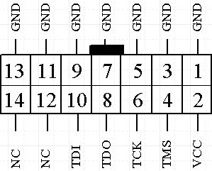
JTAG Signal Names & Description
| Pin | Signal Name | Description |
|---|---|---|
| 1 | GND | Signal ground |
| 2 | VCC(TRGT) | Target power supply |
| 3 | GND | Signal ground |
| 4 | TMS | JTAG state machine control |
| 5 | GND | Signal ground |
| 6 | TCK | Clock signal |
| 7 | GND | Signal ground |
| 8 | TDO | Data from device |
| 9 | GND | Signal ground |
| 10 | TDI | Data to device |
| 11 | GND | Signal ground |
| 12 | NC | |
| 13 | GND | Signal ground |
| 14 | NC | |
| 15 | GND | Signal ground |
JTAG Header Pinout
Development Resources
Core3S250E FPGA core board comes with a User Guide CD including development resources listed as below:
- Related software (Xilinx ISE 12 - supports Winxp/Win7, doesn't support Win8)
- Demo code (Verilog, VHDL)
- Schematic (PDF)
- FPGA development documentations
Wiki: www.waveshare.com/wiki/Core3S250E